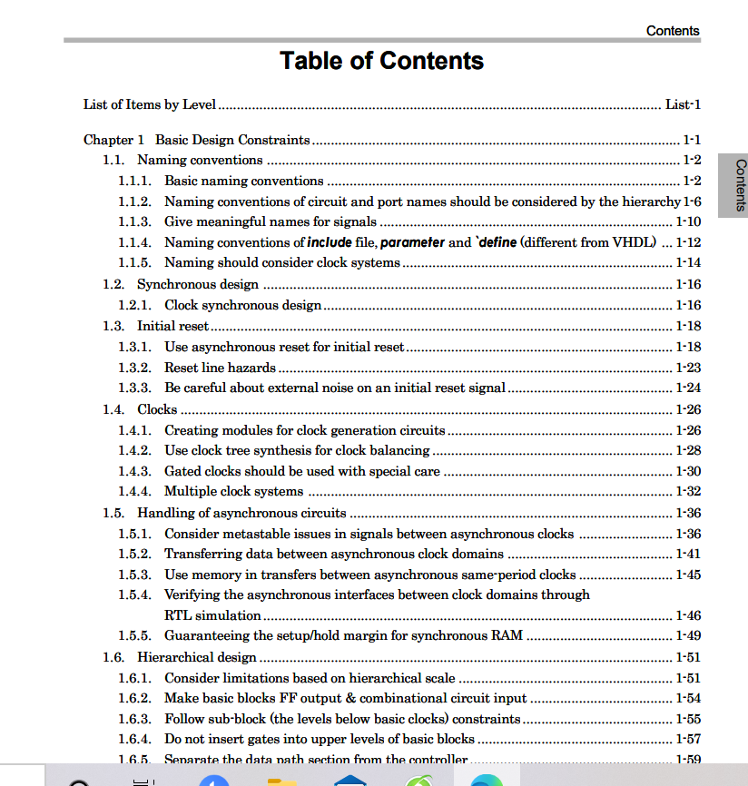
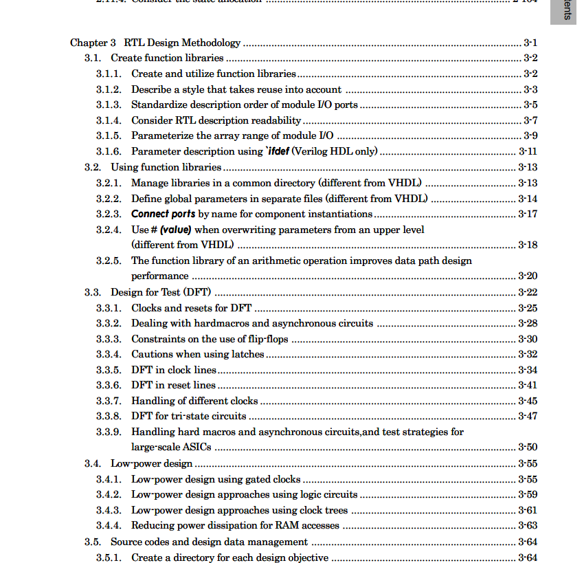
电子书-RTL Design Style Guide for Verilog HDL540页
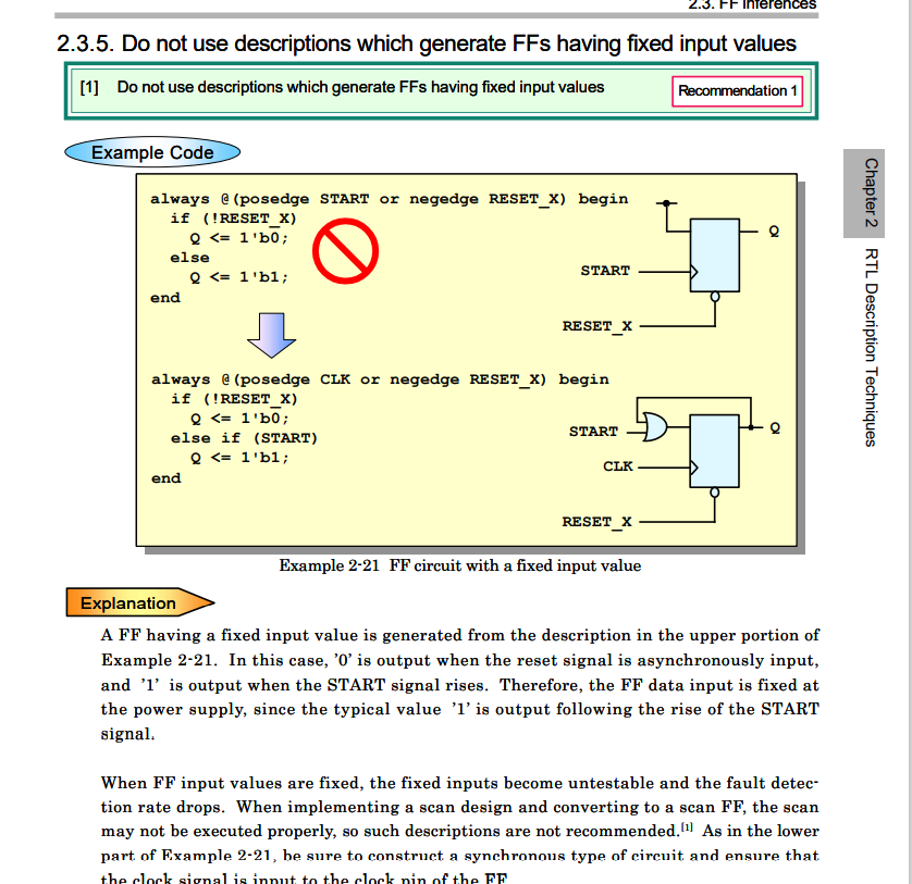
A FF having a fixed input value is generated from the description in the upper portion of Example 2-21. In this case, ’0’ is output when the reset signal is asynchronously input, and ’1’ is output when the START signal rises. Therefore, the FF data input is fixed at the power supply, since the typical value ’1’ is output following the rise of the START signal. When FF input values are fixed, the fixed inputs become untestable and the fault detection rate drops. When implementing a scan design and converting to a scan FF, the scan may not be executed properl not be executed properly, so such descriptions , so such descriptions are not are not recommended. recommended.[1] As in the lower part of Example 2-21, be sure to construct a synchronous type of circuit and ensure that the clock signal is input to the clock pin of the FF. Other than the sample shown in Example 2-21, there are situations where for certain control signals, those that had been switched due to the conditions of an external input will no longer need to be switched, leaving only a FF. If logic exists in a lower level and a fixed value is input from an upper level, the input value of the FF may also end up being fixed as the result of optimization with logic synthesis tools. In a situation like this, while perhaps difficult to completely eliminate, the problem should be avoided as much as possible.


资源简介:电子书-RTL Design Style Guide for verilog hdl540页A FF having a fixed input value is generated from the description in the upper portion of Example 2-21. In this case, ’0’ is output when the reset signal is asynchronously input, and ’1...
上传时间: 2022-03-21
上传用户:canderile
资源简介:Cadence guide for verilog
上传时间: 2013-09-04
上传用户:123454
资源简介:Cadence guide for verilog
上传时间: 2013-11-26
上传用户:daoxiang126
资源简介:原名称:CSS Cascading Style Sheets for Web Design,英文
上传时间: 2013-12-16
上传用户:yangbo69
资源简介:design guide for lcd with backlight source
上传时间: 2013-12-29
上传用户:lvzhr
资源简介:Addison.Wesley.Developing.Series.60.Applications.A.Guide.for.Symbian.OS.C.Developers.电子书,可以作为学习symbian工具书
上传时间: 2016-08-28
上传用户:myworkpost
资源简介:gps design guide,for low level study
上传时间: 2016-10-30
上传用户:liglechongchong
资源简介:some example for verilog design
上传时间: 2017-02-06
上传用户:王庆才
资源简介:ST7540 FSK powerline transceiver design guide for AMR
上传时间: 2014-01-15
上传用户:gxmm
资源简介:《Developing Series 60 Applications: A Guide for Symbian OS C++ Developers》本压缩包中包含了电子书和源码。 Series 60是在Symbian OS下进行智能手机应用程序开发的主要平台,它拥有广大的用户群。本书是诺基亚与EMCC软件公司共同推出的一本Series 60...
上传时间: 2014-11-11
上传用户:asasasas
资源简介:Securing Linux_A Survival Guide for Linux Security Version 1.0
上传时间: 2013-12-19
上传用户:aa54
资源简介:IEEE Std 1364.1-2002 IEEE Std. 1364.1 - 2002 IEEE Standard for Verilog Register Transfer Level Synthesis.rar
上传时间: 2013-12-23
上传用户:erkuizhang
资源简介:Intel® Fortran Compiler Options Quick Reference Guide for Linux Systems
上传时间: 2014-07-21
上传用户:731140412
资源简介:Programming Guide for Linux USB Device
上传时间: 2015-08-06
上传用户:稀世之宝039
资源简介:HDL Synthesizer and Optimizer Modeling Style Guide
上传时间: 2013-12-30
上传用户:ippler8
资源简介:RTL 8168/8111 Driver for Linux
上传时间: 2014-01-19
上传用户:lingzhichao
资源简介:The Windows 2000 Device Driver Book, A Guide for Programmers, Second Edition Art Baker Jerry Lozano Publisher: Prentice Hall PTR Second Edition November 20, 2000 ISBN: 0-13-020431-5, 480 pages
上传时间: 2015-09-10
上传用户:LouieWu
资源简介:The Style Guide provides you with the style specifications required to write custom reports that have a similar look to standard Microsoft CRM reports.
上传时间: 2013-12-22
上传用户:hzy5825468
资源简介:this the AVR lib who used to design the project for AVR chips
上传时间: 2015-12-10
上传用户:jing911003
资源简介:smsc911x 网卡驱动 This the users/programmers guide for the LAN911x Linux Driver The following sections can be found below * Revision History * Files * Features * Driver Parameters * Rx Performance Tuning * Tested Platforms * Rx Cod...
上传时间: 2014-12-02
上传用户:sssl
资源简介:Quick Reference for verilog hdl
上传时间: 2016-02-08
上传用户:时代电子小智
资源简介:ejtag_debug_eetimes---MIPS designer ,guide for EJTAG.
上传时间: 2014-01-04
上传用户:zmy123
资源简介:This document is an operation guide for the MPC8XXFADS board. It contains operational, functional and general information about the FADS. The MPC8XXFADS is meant to serve as a platform for s/ w and h/w development around the MPC8XX family...
上传时间: 2014-03-10
上传用户:zsjinju
资源简介:Eclipse in Action: A Guide for Web Developers by David Gallardo, Ed Burnette and Robert McGovern
上传时间: 2016-03-15
上传用户:Breathe0125
资源简介:Delphi7开发环境下的组件编写指南——Component Write s Guide for Delphi7
上传时间: 2014-01-13
上传用户:libinxny
资源简介:vi config and guide for c programmer quick guide and config
上传时间: 2016-05-13
上传用户:咔乐坞
资源简介:Quick Reference for verilog hdl
上传时间: 2014-11-29
上传用户:集美慧
资源简介:Developing.Series.60.Applications.A.Guide.for.Symbian.OS.C.Developers,学习symbian的好书
上传时间: 2016-05-29
上传用户:helmos
资源简介:java编程思想第四版课后习题答案Annotated+Solution+Guide+for+Thinking+in+Java+th+edition.rar
上传时间: 2014-12-02
上传用户:lingzhichao
资源简介:A guide for using tornado in the project and also describe the environment needed for support it.
上传时间: 2014-01-22
上传用户:caixiaoxu26